- 您现在的位置:买卖IC网 > Sheet目录333 > IRS2509SPBF (International Rectifier)IC MOSFET DRIVER
IRS2509SPbF
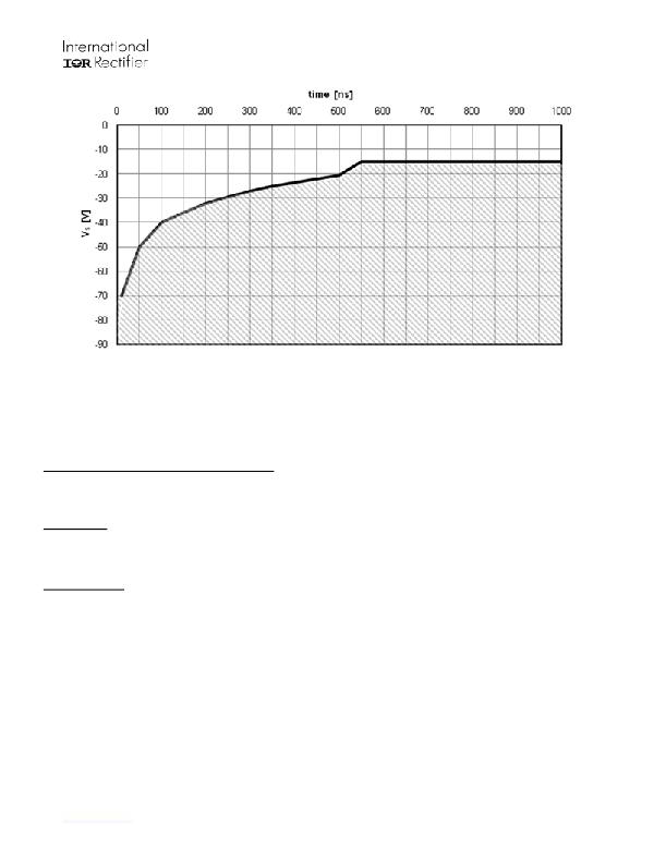
Figure 19: Negative V S transient SOA for IRS2509 @ VBS=15V
Even though the IRS2509 has been shown able to handle these large negative V S transient conditions, it is highly recommended that
the circuit designer always limit the negative V S transients as much as possible by careful PCB layout and component use.
PCB Layout Tips
Distance between high and low voltage components: It’s strongly recommended to place the components tied to the floating voltage
pins (V B and V S ) near the respective high voltage portions of the device. Please see the Case Outline information in this datasheet
for the details.
Ground Plane: In order to minimize noise coupling, the ground plane should not be placed under or near the high voltage floating
side.
Gate Drive Loops: Current loops behave like antennas and are able to receive and transmit EM noise (see Figure 20). In order to
reduce the EM coupling and improve the power switch turn on/off performance, the gate drive loops must be reduced as much as
possible. Moreover, current can be injected inside the gate drive loop via the IGBT collector-to-gate parasitic capacitance. The
parasitic auto-inductance of the gate loop contributes to developing a voltage across the gate-emitter, thus increasing the possibility
of a self turn-on effect.
www.irf.com
12
发布紧急采购,3分钟左右您将得到回复。
相关PDF资料
IRS26072DSPBF
IC DVR HI/LOW SIDE 600V 8-SOIC
IRS2607DSTRPBF
IC DVR MOSFET/IGBT N-CH 8-SOIC
IRS2608DSTRPBF
IC DRIVER MOSFET/IGBT 8-SOIC
IRS2609DSPBF
IC DVR MOSFET/IGBT N-CH 8-SOIC
IRS26302DJTRPBF
IC GATE DRIVER 3PH BRIDGE 44PLCC
IRS26310DJTRPBF
IC DRIVER MOSFET/IGBT 44-PLCC
IRS4427PBF
IC MOSFET DRIVER
IRS4427SPBF
IC DVR LOW SIDE DUAL 8-SOIC
相关代理商/技术参数
IRS2509STRPBF
功能描述:功率驱动器IC 600V 999A OTHER RoHS:否 制造商:Micrel 产品:MOSFET Gate Drivers 类型:Low Cost High or Low Side MOSFET Driver 上升时间: 下降时间: 电源电压-最大:30 V 电源电压-最小:2.75 V 电源电流: 最大功率耗散: 最大工作温度:+ 85 C 安装风格:SMD/SMT 封装 / 箱体:SOIC-8 封装:Tube
IRS2526DSPBF
功能描述:功率驱动器IC 600V Mini Ballast Controller Icr RoHS:否 制造商:Micrel 产品:MOSFET Gate Drivers 类型:Low Cost High or Low Side MOSFET Driver 上升时间: 下降时间: 电源电压-最大:30 V 电源电压-最小:2.75 V 电源电流: 最大功率耗散: 最大工作温度:+ 85 C 安装风格:SMD/SMT 封装 / 箱体:SOIC-8 封装:Tube
IRS2526DSTRPBF
功能描述:功率驱动器IC 600V Mini Ballast Controller Icr RoHS:否 制造商:Micrel 产品:MOSFET Gate Drivers 类型:Low Cost High or Low Side MOSFET Driver 上升时间: 下降时间: 电源电压-最大:30 V 电源电压-最小:2.75 V 电源电流: 最大功率耗散: 最大工作温度:+ 85 C 安装风格:SMD/SMT 封装 / 箱体:SOIC-8 封装:Tube
IRS2530
制造商:未知厂家 制造商全称:未知厂家 功能描述:DIMMING BALLAST CONTROL IC
IRS2530D
制造商:IRF 制造商全称:International Rectifier 功能描述:DIM8TM DIMMING BALLAST CONTROL IC
IRS2530DPBF
功能描述:功率驱动器IC Ballast Cntrl IC 600V .500A RoHS:否 制造商:Micrel 产品:MOSFET Gate Drivers 类型:Low Cost High or Low Side MOSFET Driver 上升时间: 下降时间: 电源电压-最大:30 V 电源电压-最小:2.75 V 电源电流: 最大功率耗散: 最大工作温度:+ 85 C 安装风格:SMD/SMT 封装 / 箱体:SOIC-8 封装:Tube
IRS2530DSPBF
功能描述:功率驱动器IC 600V DIMMING BALLAST CTRL ICR RoHS:否 制造商:Micrel 产品:MOSFET Gate Drivers 类型:Low Cost High or Low Side MOSFET Driver 上升时间: 下降时间: 电源电压-最大:30 V 电源电压-最小:2.75 V 电源电流: 最大功率耗散: 最大工作温度:+ 85 C 安装风格:SMD/SMT 封装 / 箱体:SOIC-8 封装:Tube
IRS2530DSTRPBF
功能描述:功率驱动器IC Ballast Cntrl IC 600V .500A RoHS:否 制造商:Micrel 产品:MOSFET Gate Drivers 类型:Low Cost High or Low Side MOSFET Driver 上升时间: 下降时间: 电源电压-最大:30 V 电源电压-最小:2.75 V 电源电流: 最大功率耗散: 最大工作温度:+ 85 C 安装风格:SMD/SMT 封装 / 箱体:SOIC-8 封装:Tube
